Power diode, power transistor, gate-controlled switch, Gate
Controlled Switch (Gate-turn-off SCR) GCS (GTO) and
programmable unijunction transistor.
ELECTRONIC CONTROL DEVICES (PART 1)
General objective : To apply the concept of electronic control devices.
Specific objectives : At the end of the unit you should be able to:
- Identify the power of diodes
- Define the symbol of diodes
- List the types of diodes
- Define the characteristics of diodes
- Define the application of diodes
- Draw the construction of diodes
- Identify the power transistor concept
5.1 INTRODUCTION OF POWER DIODE
A diode is a component that allows current to freely flow through it in one direction but essentially stops any current from flowing in the reverse direction. Power diodes can be assumed as ideal switches for most applications but practical diodes differ from the ideal characteristics and have certain limitations. The power diodes are similar to pn-junction signal diodes.
5.2 PRINCIPLE AND CONSTRUCTION OF DIODE
According to the introduction above, you can see that a PN junction has all the characteristics of a diode. Thus, from previous discussion on the PN junction, its characteristics apply to the diode. The legend for Fig. 5.2(a) could just as well be “ capacitance of a reverse-biased diode”.

Nearly all diodes used in electronics today are silicon PN junctions. Silicon is preferred because of its low current leakage. There are also a few diodes made from germanium PN junctions. They are primarily used when the lower potential barrier voltage of the germanium junction is advantageous.
Figure 5.2 (b) shows a cutaway view of a typical diode that is capable of carrying 2 A of current. One of the diode leads connects to the P-type material and the other to the N-type material. The silicon PN junction is very small: about the diameter of the lead wire and a few thousands of an inch thick. The body of the of this plastic-encased diode is about 1/8 inch in diameter and about 5/16 inch long. The band of the left end of the body identifies the cathode end of the diode. The cathode end of a diode is N-type material and the anode end is always P-type material. Thus, for a forward-bias diode, the anode must be positive to the cathode.

5.3 SYMBOL OF DIODES.
The schematic symbol for diode is shown in figure 5. 3 (a). The cathode is represented by the vertical straight line and the anode by the triangle. Figure 5.3 (b) and 5.3 (c) illustrate forward-biasing and reverse-biasing respectively.

5.4 TYPES OF POWER DIODES

Ideally, a diode should have no reverse recovery time. However, the manufacturing cost of such a diode will increase. In many applications, the effects of reverse recovery time will not be significant, and inexpensive diodes can be used. Depending on the recovery characteristics and manufacturing techniques, the power diodes can be classified into three categories. The characteristics and practical limitations of each type restrict their applications:
a. Standard or general-purpose diodes
b. Fast-recovery diodes
c. Schottky diodes
5.4.1 Standard or general-purpose diodes.
The general-purpose rectifier diodes have relatively high reverse recovery time, typically 25 µs, and are used in low-speed applications, where recovery time is not critical. These diodes cover current rating from less than 1 A to several thousands of amperes, with voltage ratings from 50 V to around 5 kV. These diodes are generally manufactured by diffusion. However, alloyed types of rectifiers that are used in welding power supplies are most cost-effective and rugged, and their ratings can go up to 300 A and 1000 V.
5.4.2 Fast-recovery diodes
The fast-recovery diodes have low recovery time, normally less than 5 µs. They are used in dc-dc and dc-ac converter circuits, where the speed of recovery is often of critical importance. These diodes cover current ratings from less than 1 A to hundreds of amperes, with voltage ratings from 50 V to around 3 kV.
For voltage ratings above 400V, fast-recovery diodes are generally made by diffusion and the recovery time is controlled by platinum or gold diffusion. For voltage ratings below 400V, epitaxial diodes provide faster switching speeds than that of diffused diodes. The epitaxial diodes have a narrow base width, resulting in a fast recovery time of as low as 50 ns. Fast-recovery diodes of various sizes are shown in Figure 5.4.2.

5.4.3 Schottky diodes
The charge storage problem of a pn-junction can be eliminated (or minimized) in a Schottky diode. It is accomplished by setting up a “ barrier potential” with a contact between a metal and a semiconductor. A layer of metal is deposited on a thin epitaxial layer of n-type silicon. The potential barrier simulates the behavior of a pn-junction. The rectifying action depends on the majority carriers only, and as a result there are no excess minority carriers to recombine. The recovery effect is due solely to the self-capacitance of the semiconductor junction.
The recovered charge of a Schottky diode is much less than that of an equivalent pn-junction diode. Since it is due only to the junction capacitance, it is largely independent of the reverse di/dt. A Schottky diode has a relatively low forward voltage drop.

5.5 CHARACTERISTICS OF DIODE
5.5.1 Peak Inverse Voltage
A diode can withstand only so much inverse voltage before it breaks down. The peak inverse voltage (PIV) ranges from 50 V to 4000 V, depending of the construction. If the rated PIV is exceeded, the diode begins to conduct in reverse and in many cases, is immediately destroyed.
5.5.2 Maximum Average Current
There is also a limit to the average current a diode can carry. The maximum current may range from a few hundred milliamperes to over 4000 A, depending of construction and size of the diode. The nominal current rating depends upon the temperature of the diode, which, in turn, depend upon the way it is mounted and how it is cooled.
5.5.3 Maximum Temperature
The
voltage across a diode times the current it carries is equal to the power lost,
which is entirely converted into heat. The resulting temperature rise of the
diode must never exceed the permissible
limits, otherwise the diode will be destroyed.
5.6 APPLICATION OF DIODES.
Diodes have many applications, some of which are
found again and again, in one form or
another, in electronic power circuit. In the sections that follow, we will
analyze a few circuit that involve only diodes. They will illustrate the
methodology of power circuit analysis while revealing some basic principles
common to many industrial applications. Examples of the applications are :
a.
battery changer with series resistor
b.
battery changer with series inductor
c.
single-phase bridge
rectifier
d.
filter
e.
three-phase, 3-pulse diode rectifier
f.
three-phase, 6-pulse diode rectifier
g.
effective line current: fundamental line current
h.
distortion power factor
i.
displacement power factor harmonic content
5.7
POWER TRANSISTORS
Power transistors
have controlled turn-on and turn-off characteristics. The transistors, which
are used as switching elements, are operated in the saturation region,
resulting in a low on-state voltage drop. The switching speed of modern
transistors is much higher than that of thyristors and they are extensively
employed in dc-dc and dc-ac converters, with inverse parallel-connected diodes
to provide bidirectional current flow. However, their voltage and current
ratings are lower than those of thyristors and transistors are normally used in
low to medium power applications. The power transistors can be classified
broadly into four categories:
1.
Bipolar junction transistors (BJTs)
2.
Metal-oxide-semiconductor field-effect transistors
(MOSFET)
3.
Static induction transistors (SITs)
4. Insulated-gate bipolar transistors (IGBTs)
BJTs or MOSFETs,
SITs or IGBTs, can be assumed as ideal switches to explain the power conversion
techniques. A transistor switch is much simpler than a forced-commutated
thyristor switch. However, the choice between a BJT and a MOSFET in the
converter circuits is not obvious, but either of them can replace a thyristor,
provided that their voltage and current ratings meet the output requirements of the converter. Practical transistors differ from ideal devices. The transistors
have certain limitations and are restricted to some applications. The characteristics
and ratings of each type should be examined to determine its suitability to a
particular application.
A bipolar transistor is formed by adding a
second p- or n-region to a pn-junction
diode. With two n-regions and one p-region, two junctions are formed and it is
known as an NPN-transistor, as shown in
Fig. 5.7 (a). With two p-regions and
one n-region, it is called as a PNP-transistor, as shown in Fig 5.7 (b).
The three terminals are named as collector, emitter, and base. A bipolar transistor has two junctions,
collector-base junction (CBJ) and base-emitter junction (BEJ). NPN-transistors of various sizes are
shown in Fig 5.7 (c).


A GTO has low gain during turn-off, typically 6, and requires
a relatively high negative current pulse to turn off. It has higher on-state
voltage than that of SCRs. The on-state voltage of a typical 550-A 1200-V
GTO is typically 3.4 V. A
160-A 200-V GTO of type 160PFT is shown in Fig. 6.3.

The programmable
unijunction transistor (PUT) is small thyristor shown in Fig. 6.4(a). A PUT can
be used as a relaxation oscillator as shown in Fig. 6.4(b). The gate voltage VG is maintained from the supply
by the resistor divider R1
and R2, and determines
the peak voltage Vp. In
the case of the UJT, Vp
is fixed for device by the dc supply voltage. But Vp of a PUT can be varied by varying the resistor
divider R1 and R2. If the anode voltage VA is less than the gate voltage VG, the device will remain in its off-state. If VA exceeds the gate voltage by one diode forward voltage VD, the peak point is reached
and the device turns on. The peak current Ip and the
valley point current Iv both depend on the
equivalent impedance on the gate RG = R1 R2 /( R1
+ R2) and the dc
supply voltage Vs. in general , Rk is limited to a value below 100 Ω.


The
unijunction transistor (UJT) is commonly used for generating triggering signals
for SCRs. A basic UJT-triggering circuit is shown in Fig. 6.5(a). A UJT has three terminals, called the emitter
E, base-one B1,
and base-two B2.
Between B1 and
B2 the
unijunction has the characteristics of an ordinary resistance. This resistance
is the interbase resistance RBB and has values in the range 4.7 to 9.1 kΩ. The static
characteristics of a UJT are shown in Fig. 6.5(b). When the dc supply voltage
Vs is applied, the capacitor C is charged through resistor R since the emitter
circuit of the UJT is in the open state. The time constant of the charging circuit
is T1 = RC. When
the emitter voltage VE, which is the same
as the capacitor voltage vc , reaches the peak voltage Vp, the UJT turns on and capacitor C will discharge through RB1 at a determined by the time constant T2 = RB1C. T2 is much smaller than T1. When the emitter voltage VE decays to the valley point Vv, the emitter ceases to conduct, the
UJT turns off, and the charging cycle is repeated. The waveforms of the emitter
and triggering voltages are shown in Fig. 6.5 (c).


5.7
STEADY-STATE
CHARACTERISTICS
Although there are three possible configurations--
common-collector, common base, and common-emitter, the common-emitter
configuration, which is shown in Fig. 5.8(a) for an NPN-transistor, is generally used in switching applications. The
typical input characteristics of base current, IB, against base-emitter
voltageVBE, are shown in Fig. 5.8(b). Figure 5.8 (c) shown the typical output characteristics of collector
current, Ic, against
collector-emitter voltage, VcE. For a
PNP-transistor, the polarities of all currents and voltages are reversed.
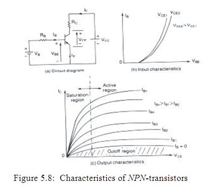
There are three operating regions of a
transistor: cutoff, active, and saturation. In the cutoff region, the
transistor is off or the base current is not enough to turn it on and both
junctions are reverse biased. In the active region, the transistor acts as an
amplifier, where the collector current is amplified by a gain and the
collector-emitter voltage decreases with the base current. The CBJ is reverse
biased, and the BEJ is forward biased. In the saturation region, the base
current is sufficiently high so that the collector-emitter voltage is low, and
the transistor acts as a switch. Both junctions (CBJ and BEJ) are forward
biased. The transfer characteristic, which is a plot of VCE against IB, is shown in Fig
5.8(d).

ELECTRONIC CONTROL DEVICES (PART 2)
General objective : To understand the concept of electronic
control devices.
Specific objectives : At
the end of the unit you should be able to:
- Identify the Phase-Control Thyristors
- Identify the Gate-Turn-Off Thyristors
- Define the symbol of GTO
- Identify the Programmable Unijunction Transistor (PUT)
- Define the symbol of PUT
- Identify the Uni-junction Transistor (UJT)
6.1 PHASE-CONTROL THYRISTORS
(SCRs)
This type of
thyristors generally operates at the line frequency and is turned off by
natural commutation. The turn-off time,tq,
is of the order of 50 to 100 µs. This is most suited for low-speed switching
applications and is also known as converter thyristor. Since a thyristor is
basically a silicon-made controlled device, it is also known as
silicon-controlled rectifier (SCR).
The
on-state voltage , VT,
varies typically from about 1.15 V for 600 V to 2.5 V for 4000 V devices; and
for a 5500-A 1200-V thyristor it is
typically 1.25 V. The modern thyristors
use an amplifying gate, where an auxiliary thyristor TA is
gated on by a gate signal and then the amplified output of TA
is applied as a gate signal to the main thyristor TM. This shown in Fig. 6.1. The
amplifying gate permits high dynamic characteristics with typical dv/dt of
1000 V/µs and di/dt of 500 A/µs and simplifies the circuit design by
reducing or minimizing di/dt limiting inductor and dv/dt protection circuits.
6.2 THYRISTOR TURN-OFF
A
thyristor which is in the on-state can be turned off by reducing the forward
current to a level below the holding current IH. There are various techniques for turning off a
thyristor. In all the commutation techniques, the anode current is maintained
below the holding current for a sufficiently long time, so that all the excess
carriers in the four layers are swept out or recombined.
6.3 GATE-TURN-OFF THYRISTOR
A gate-turn-off
thyristor (GTO) like an SCR can be turned on by applying a positive gate
signal. However, it can be turned off by a negative gate signal. A GTO is a
latching device and can be built with current and voltage ratings similar to
those of an SCR. A GTO is turned on by applying a short positive pulse and
turned off by a short negative pulse to its gate. The GTOs have advantages over
SCRs: (1) elimination of commutating
components in forced commutation, resulting in reduction in cost, weight, and
volume; (2) reduction in acoustic and
electromagnetic noise due to the elimination of commutation chokes; (3) faster
turn-off, permitting high switching frequencies; and (4) improved efficiency of
converters.
In low-power
applications, GTOs have the following advantages over bipolar transistors: (1)
a higher blocking voltage capability; (2) a high ratio of peak controllable
current to average current; (3) a high ratio of peak surge current to average
current, typically 10:1; (4) a high
on-state gain (anode current/gate current), typically 600; and (5) a pulsed
gate signal of short duration. Under surge conditions, a GTO goes into deeper
saturation due to regenerative action.
On the other hand, a bipolar transistor tends to come out of saturation.

6.3 PROGRAMMABBLE UNIJUNCTION TRANSISTOR
(PUT)


6.5 UNIJUNCTION TRANSISTOR
(UJT)


